Skip to content
AZITECH-LOGO
  • Home
  • PCB Services
    • PCB Layout Service
      • Design for manufacturing
      • PCB Design Center
      • Preference Centre
    • Prototypes
      • PCB Compliance
      • Delivery
    • Volumes
      • Warehousing
      • Data Security
  • News & Events
    • News
    • Events
  • About
    • Who are we
    • Contact us
Home
PCB Services
PCB Layout Service
Design for manufacturing
PCB Design Center
Preference Centre
Prototypes
PCB Compliance
Delivery
Volumes
Warehousing
Data Security
News & Events
News
Events
About
Who are we
Contact us

How to avoid issues with Stacked vias

Home
News
How to avoid issues with Stacked vias
byRobert Ludvigsen

Stacked vias and how to plan for success.

Stacked vias are commonly utilized in the electronics industry to maximize functionality within limited space, often allowing for the integration of more features while reducing the number of layers required compared to traditional vias.

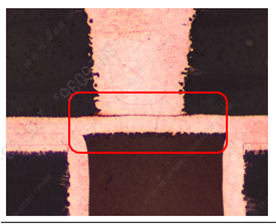
The accompanying image depicts a cross-section of a stacked micro via positioned atop a mechanically drilled via, which is subsequently filled and plated. This configuration can occasionally lead to cracks in the joint connection.

This issue is well-recognized within the PCB industry, and various explanations, often myth-based, attempt to elucidate its causes. In some instances, the occurrence may be attributed to suboptimal PCB design choices, while in others, it could result from inadequate handling of this technology by the PCB manufacturer.

PCB compliance for stacked vias
Achieving compliance with HDI (High-Density Interconnect) boards incorporating stacked vias requires careful consideration and collaboration between PCB designers and manufacturers. Design choices made by the PCB designer play a critical role in setting up the PCB factory for success. Selection of appropriate materials and technologies must align with the specific parameters outlined by the PCB factory.

At Azitech, we’ve observed instances where PCB compliance at this level has been compromised by EMS factories or PCB purchasers aiming to reduce costs. To ensure maximum reliability, a deeper partnership with the PCB factory is essential, involving a thorough understanding of their machinery and processes. This collaboration is pivotal in distinguishing between success and failure.

Alert to all Original Equipment Manufacturers (OEMs)
Not all PCB factories possess comprehensive control over the factors influencing the reliability of stacked vias. Some may neglect proper maintenance practices, yet still accept orders despite potential mismatches between factory capabilities and the choices made by the PCB designer. While a PCB factory’s lack of knowledge or experience in producing PCBs with stacked vias may not immediately disqualify them, final approval may only be provisional. Failures may occur during assembly or subsequent operations at the end customer, highlighting the importance of thorough testing and caution.

An alternative to stacked vias is staggered vias, which generally offer greater durability. However, this option may not always be feasible, especially when employing Micro BGAs (Ball Grid Arrays).

Azitech PCB recommendations for PCBs stacked viasIf stacked vias are used on PCB materials with high CTE-z (Coefficient of Thermal Expansion in the Z-axis) values, several issues may arise:
1. Thermal Stress: PCB materials with high CTE-z values tend to expand and contract more significantly in the Z-axis direction when exposed to temperature variations. Stacked vias, especially those with different plating materials or diameters, can exacerbate the thermal stress. The differential expansion and contraction between the vias and the surrounding material can lead to mechanical stress concentration, which may cause via cracking, solder joint failures, or delamination issues.
2. Reliability concerns: The excessive thermal stress caused by using stacked vias on high CTE-z materials can compromise the integrity and long-term reliability of the PCB. Over time, the repeated thermal cycling can induce fatigue in the vias and surrounding materials, leading to electrical failures and reduced lifespan.
3. Warpage and Distortion: High CTE-z materials are prone to warping or bowing when exposed to thermal stress. The use of stacked vias can aggravate this effect, leading to uneven board surfaces, difficulty in mounting components, and potential assembly issues.
4. Signal Integrity: The differential expansion and contraction caused by high CTE-z materials can negatively impact signal integrity. Stacked vias may experience changes in impedance due to the varying dimensions and material characteristics, leading to signal distortion, reflection, or impedance mismatch.
To mitigate these issues, it is essential to consider several approaches:
1. Material Selection: Choose PCB materials with lower CTE-z values that are better matched to the CTE of the stacked vias and other components on the board. Selecting materials with a more balanced CTE can minimize the differential expansion and reduce the stress on the vias.
2. Design Optimization: Optimize the via placement to minimize the differential thermal stress across the board. Use techniques such as via staggering, via stitching, or reducing the number of stacked vias to alleviate stress concentration.
3. Thermal Management: Implement adequate thermal management techniques, including thermal vias, heat sinks, and proper component placement to distribute heat and minimize hotspots. Effective heat dissipation can help reduce the thermal stress on the stacked vias.
4. Reliability Testing: Perform thorough validation and reliability testing to assess the performance and durability of the PCB under different thermal cycling conditions. This testing will help identify issues early on and enable necessary design improvements.
By carefully considering material selection, design optimization, thermal management, and thorough testing, the challenges associated with using stacked vias on high CTE-z materials can be mitigated, leading to improved reliability and performance of the PCB.

Sources:

https://resources.altium.com/p/ipc-warning-about-microvia-reliability-high-performance-products
https://iconnect007.com/index.php/article/115926/ipc-issues-warning-on-microvia-reliability-for-high-performance-products/115929?skin=pcb

Share this post:

latest news

Connecting Global Electronics Minds: Highlights from Our Science based PCB Design Seminar

Azitech Technical Update: Choosing the Best PCB Surface Finish

Quality at Our Core – Insights from Our June 2025 Audit 

Azitech RapidX – Drone delivery.

How to avoid issues with Stacked vias

Related News:

Connecting Global Electronics Minds: Highlights from Our Science based PCB Design Seminar
Seminar Poster
Connecting Global Electronics Minds — Azitech PCB Seminar Highlights In two action-packed days our international...
Read More
Connecting Global Electronics Minds: Highlights from Our Science based PCB Design Seminar
Connecting Global Electronics Minds — Azitech PCB Seminar Highlights In two action-packed days our international PCB seminar brought together 50+ delegates from 20+ companies across 10+ countries for focused knowledge sharing, product demos and partnership building. The goal was simple: accelerate practical PCB design know-how, spark cross-border electronics collaboration, and showcase real-world tools and workflows...
Seminar Poster
Connecting Global Electronics Minds: Highlights from Our Science based PCB Design Seminar
Seminar Poster
Connecting Global Electronics Minds — Azitech PCB Seminar Highlights In two action-packed days our international...
Read More
Azitech Technical Update: Choosing the Best PCB Surface Finish
image (1)
Azitech’s technical update explains why PCB surface finishes matter and compares ENIG, OSP, Immersion Silver,...
Read More
Azitech Technical Update: Choosing the Best PCB Surface Finish
Azitech’s technical update explains why PCB surface finishes matter and compares ENIG, OSP, Immersion Silver, ENEPIG, and LF-HASL. Learn the pros/cons of each finish and key selection criteria to prevent copper oxidation and ensure reliable solder joints. Here’s the thing: exposed copper on a PCB oxidizes almost instantly when it hits air. That oxidation? It...
image (1)
Azitech Technical Update: Choosing the Best PCB Surface Finish
image (1)
Azitech’s technical update explains why PCB surface finishes matter and compares ENIG, OSP, Immersion Silver,...
Read More
Quality at Our Core – Insights from Our June 2025 Audit 
Screenshot 2025-11-03 at 1.22.16 PM
Ensuring Quality through Rigorous Audits At Azitech, quality isn’t just a word – it’s a promise...
Read More
Quality at Our Core – Insights from Our June 2025 Audit 
Ensuring Quality through Rigorous Audits At Azitech, quality isn’t just a word – it’s a promise we uphold every day. We work with state-of-the-art partners and audited factories to guarantee your PCB projects meet the highest standards.   In June 2025, we conducted an in-depth audit of our European Factory, covering everything from machinery and clean-room...
Screenshot 2025-11-03 at 1.22.16 PM
Quality at Our Core – Insights from Our June 2025 Audit 
Screenshot 2025-11-03 at 1.22.16 PM
Ensuring Quality through Rigorous Audits At Azitech, quality isn’t just a word – it’s a promise...
Read More
Azitech RapidX – Drone delivery.
Drone-delivery-Azitech
Azitech ApS – Secure PCB Connections We are beyond excited to announce our most ambitious...
Read More
Azitech RapidX – Drone delivery.
Azitech ApS – Secure PCB Connections We are beyond excited to announce our most ambitious logistics initiative yet: Azitech RapidX – Europe’s first PCB production and delivery system combining 24-hour manufacturing with 3-hour drone drop-off anywhere in Europe. Yes, you read that right: Gerber in today. Assembled, tested, and drone-delivered tomorrow.Through our new partnership with...
Drone-delivery-Azitech
Azitech RapidX – Drone delivery.
Drone-delivery-Azitech
Azitech ApS – Secure PCB Connections We are beyond excited to announce our most ambitious...
Read More
How to avoid issues with Stacked vias
Stacked via crack
Stacked vias and how to plan for success. Stacked vias are commonly utilized in the...
Read More
How to avoid issues with Stacked vias
Stacked vias and how to plan for success. Stacked vias are commonly utilized in the electronics industry to maximize functionality within limited space, often allowing for the integration of more features while reducing the number of layers required compared to traditional vias. The accompanying image depicts a cross-section of a stacked micro via positioned atop...
Stacked via crack
How to avoid issues with Stacked vias
Stacked via crack
Stacked vias and how to plan for success. Stacked vias are commonly utilized in the...
Read More
Welcome to Martin Raunsbæk Jørgensen
Martin
Martin has joined Azitech on the 1st of February 2024, where he started as Azitech’s...
Read More
Welcome to Martin Raunsbæk Jørgensen
Martin has joined Azitech on the 1st of February 2024, where he started as Azitech’s Key Account Manager for Fyn, Jylland and Norway. He will primarily work from his office in Aarhus, where he will provide his extensive PCB consultancy to the territory. Martin has many years of experience with electronic manufacturing, and we look...
Martin
Welcome to Martin Raunsbæk Jørgensen
Martin
Martin has joined Azitech on the 1st of February 2024, where he started as Azitech’s...
Read More

Post navigation

Welcome to Martin Raunsbæk Jørgensen
Azitech RapidX – Drone delivery.

Join Our Newsletter

Dont miss out on our latest news, product releases and guides.

PCB technologies

  • PCB Production
  • PCB Compliance
  • Data Security
  • PCB Design
  • PCB Layout
  • Preference Centre

Resources

  • Design Center
  • Events
  • News

Who we are

  • Meet The Team
  • About
  • Contact
  • Careers
  • Privacy Policy

Newsletter

Subscribe to our sales newsletter to stay up to date with our latest products and services.

AZITECH-LOGO
© Azitech 2023, All rigths reserved

Azitech ApS ● Industrivej 2, 5550 Langeskov, Denmark ● CVR: 29417717

  • Office hours Mon - Fri 08.00 - 16.00
  • Tel: +45 6613 0768
  • Email: support@azitech.dk
Facebook-f Linkedin Youtube

Powered by azitech.dk

Azitech ApS ● Industrivej 2, 5550 Langeskov, Denmark ● CVR: 29417717

  • Office hours Mon - Fri 08.00 - 16.00
  • Tel: +45 6613 0768
  • Email: support@azitech.dk
AZITECH-LOGO
© Azitech 2023, All rigths reserved
Facebook-f Linkedin Youtube

designed by adtify.dk