Stacked vias and how to plan for success.
Stacked vias are commonly utilized in the electronics industry to maximize functionality within limited space, often allowing for the integration of more features while reducing the number of layers required compared to traditional vias.
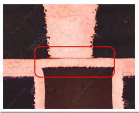
 The accompanying image depicts a cross-section of a stacked micro via positioned atop a mechanically drilled via, which is subsequently filled and plated. This configuration can occasionally lead to cracks in the joint connection.
This issue is well-recognized within the PCB industry, and various explanations, often myth-based, attempt to elucidate its causes. In some instances, the occurrence may be attributed to suboptimal PCB design choices, while in others, it could result from inadequate handling of this technology by the PCB manufacturer.
PCB compliance for stacked vias
Achieving compliance with HDI (High-Density Interconnect) boards incorporating stacked vias requires careful consideration and collaboration between PCB designers and manufacturers. Design choices made by the PCB designer play a critical role in setting up the PCB factory for success. Selection of appropriate materials and technologies must align with the specific parameters outlined by the PCB factory.
At Azitech, we’ve observed instances where PCB compliance at this level has been compromised by EMS factories or PCB purchasers aiming to reduce costs. To ensure maximum reliability, a deeper partnership with the PCB factory is essential, involving a thorough understanding of their machinery and processes. This collaboration is pivotal in distinguishing between success and failure.
Alert to all Original Equipment Manufacturers (OEMs)
Not all PCB factories possess comprehensive control over the factors influencing the reliability of stacked vias. Some may neglect proper maintenance practices, yet still accept orders despite potential mismatches between factory capabilities and the choices made by the PCB designer. While a PCB factory’s lack of knowledge or experience in producing PCBs with stacked vias may not immediately disqualify them, final approval may only be provisional. Failures may occur during assembly or subsequent operations at the end customer, highlighting the importance of thorough testing and caution.
An alternative to stacked vias is staggered vias, which generally offer greater durability. However, this option may not always be feasible, especially when employing Micro BGAs (Ball Grid Arrays).
Azitech PCB recommendations for PCBs stacked viasIf stacked vias are used on PCB materials with high CTE-z (Coefficient of Thermal Expansion in the Z-axis) values, several issues may arise:
1. Thermal Stress: PCB materials with high CTE-z values tend to expand and contract more significantly in the Z-axis direction when exposed to temperature variations. Stacked vias, especially those with different plating materials or diameters, can exacerbate the thermal stress. The differential expansion and contraction between the vias and the surrounding material can lead to mechanical stress concentration, which may cause via cracking, solder joint failures, or delamination issues.
2. Reliability concerns: The excessive thermal stress caused by using stacked vias on high CTE-z materials can compromise the integrity and long-term reliability of the PCB. Over time, the repeated thermal cycling can induce fatigue in the vias and surrounding materials, leading to electrical failures and reduced lifespan.
3. Warpage and Distortion: High CTE-z materials are prone to warping or bowing when exposed to thermal stress. The use of stacked vias can aggravate this effect, leading to uneven board surfaces, difficulty in mounting components, and potential assembly issues.
4. Signal Integrity: The differential expansion and contraction caused by high CTE-z materials can negatively impact signal integrity. Stacked vias may experience changes in impedance due to the varying dimensions and material characteristics, leading to signal distortion, reflection, or impedance mismatch.
To mitigate these issues, it is essential to consider several approaches:
1. Material Selection: Choose PCB materials with lower CTE-z values that are better matched to the CTE of the stacked vias and other components on the board. Selecting materials with a more balanced CTE can minimize the differential expansion and reduce the stress on the vias.
2. Design Optimization: Optimize the via placement to minimize the differential thermal stress across the board. Use techniques such as via staggering, via stitching, or reducing the number of stacked vias to alleviate stress concentration.
3. Thermal Management: Implement adequate thermal management techniques, including thermal vias, heat sinks, and proper component placement to distribute heat and minimize hotspots. Effective heat dissipation can help reduce the thermal stress on the stacked vias.
4. Reliability Testing: Perform thorough validation and reliability testing to assess the performance and durability of the PCB under different thermal cycling conditions. This testing will help identify issues early on and enable necessary design improvements.
By carefully considering material selection, design optimization, thermal management, and thorough testing, the challenges associated with using stacked vias on high CTE-z materials can be mitigated, leading to improved reliability and performance of the PCB.
Sources:
https://resources.altium.com/p/ipc-warning-about-microvia-reliability-high-performance-products
https://iconnect007.com/index.php/article/115926/ipc-issues-warning-on-microvia-reliability-for-high-performance-products/115929?skin=pcb